
![]()
Let’s Get It Started!
This user guide uses the NEORV32 project as is from the official neorv32 repository.
To make your first NEORV32 project run, follow the guides from the upcoming sections. It is recommended to
follow these guides step by step and eventually in the presented order.
This guide uses the minimalistic and platform/toolchain agnostic SoC test setups from
rtl/test_setups for illustration. You can use one of the provided test setups for
your first FPGA tests. Alternatively, have a look at the setups folder,
which provides more sophisticated example setups for various FPGAs/FPGA boards and toolchains.
|
1. Software Toolchain Setup
To compile (and debug) executables for the NEORV32 a RISC-V toolchain is required. There are two possibilities to get this:
-
Download and build the official RISC-V GNU toolchain yourself.
-
Download and install a prebuilt version of the toolchain; this might also done via the package manager / app store of your OS
The default toolchain prefix (RISCV_PREFIX variable) for this project is riscv32-unknown-elf-. Of course you can use any other RISC-V
toolchain (like riscv64-unknown-elf-) that is capable to emit code for a rv32 architecture. Just change RISCV_PREFIX
according to your needs.
|
1.1. Building the Toolchain from Scratch
To build the toolchain by yourself you can follow the guide from the official https://github.com/riscv-collab/riscv-gnu-toolchain GitHub page.
You need to make sure the generated toolchain fits the architecture of the NEORV32 core. To get a toolchain that even supports minimal
ISA extension configurations, it is recommend to compile for rv32i only. Please note that this minimal ISA also provides further ISA
extensions like m or c. Of course you can use a multilib approach to generate toolchains for several target ISAs at once.
rv32i (minimal ISA)riscv-gnu-toolchain$ ./configure --prefix=/opt/riscv --with-arch=rv32i --with-abi=ilp32
riscv-gnu-toolchain$ make
Keep in mind that - for instance - a toolchain build with --with-arch=rv32imc only provides library code compiled with
compressed (C) and mul/div instructions (M)! Hence, this code cannot be executed (without
emulation) on an architecture without these extensions!
|
1.2. Downloading and Installing a Prebuilt Toolchain
Alternatively, you can download a prebuilt toolchain.
1.2.1. Use The Toolchain I have Build
I have compiled a GCC toolchain on a 64-bit x86 Ubuntu (Ubuntu on Windows, actually) and uploaded it to GitHub. You can directly download the according toolchain archive as single zip-file within a packed release from https://github.com/stnolting/riscv-gcc-prebuilt.
Unpack the downloaded toolchain archive and copy the content to a location in your file system (e.g.
/opt/riscv). More information about downloading and installing my prebuilt toolchains can be found in
the repository’s README.
1.2.2. Use a Third Party Toolchain
Of course you can also use any other prebuilt version of the toolchain. There are a lot RISC-V GCC packages out there - even for Windows. On Linux system you might even be able to fetch a toolchain via your distribution’s package manager.
Make sure the toolchain can (also) emit code for a rv32i architecture, uses the ilp32 or ilp32e ABI and was not build using
CPU extensions that are not supported by the NEORV32 (like D).
|
1.3. Installation
Now you have the toolchain binaries. The last step is to add them to your PATH environment variable (if you have not
already done so): make sure to add the binaries folder (bin) of your toolchain.
$ export PATH:$PATH:/opt/riscv/binYou should add this command to your .bashrc (if you are using bash) to automatically add the RISC-V
toolchain at every console start.
1.4. Testing the Installation
To make sure everything works fine, navigate to an example project in the NEORV32 example folder and execute the following command:
neorv32/sw/example/blink_led$ make checkThis will test all the tools required for generating NEORV32 executables.
Everything is working fine if Toolchain check OK appears at the end.
2. General Hardware Setup
This guide shows the basics of setting up a NEORV32 project for FPGA implementation (or simulation only) from scratch. It uses a simplified test "SoC" setup of the processor to keeps things simple at the beginning. This simple setup is intended for evaluation or as "hello world" project to check out the NEORV32 on your FPGA board.
If you want to use a more sophisticated pre-defined setup to start with, check out the
setups folder, which provides example setups for various FPGA, boards and toolchains.
|
The NEORV32 project features two minimalistic pre-configured test setups in
rtl/test_setups.
Both test setups only implement very basic processor and CPU features.
The main difference between the two setups is the processor boot concept - so how to get a software executable
into the processor:
-
rtl/test_setups/neorv32_testsetup_approm.vhd: this setup does not require a connection via UART. The software executable is "installed" into the bitstream to initialize a read-only memory. Use this setup if your FPGA board does not provide a UART interface. -
rtl/test_setups/neorv32_testsetup_bootloader.vhd: this setups uses the UART and the default NEORV32 bootloader to upload new software executables. Use this setup if your board does provide a UART interface.
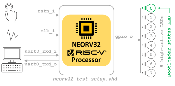
rtl/test_setups/neorv32_testsetup_bootloader.vhd)|
External Clock Source
These test setups are intended to be directly used as design top entity. Of course you can also instantiate them
into another design unit. If your FPGA board only provides very fast external clock sources (like on the FOMU board)
you might need to add clock management components (PLLs, DCMs, MMCMs, …) to the test setup or to the according top entity
if you instantiate one of the test setups.
|
-
Create a new project with your FPGA EDA tool of choice.
-
Add all VHDL files from the project’s
rtl/corefolder to your project.
|
Internal Memories
For a general first setup (technology-independent) use the *.default.vhd memory architectures for the internal memories
(IMEM and DMEM). These are located in rtl/core/mem so make sure to add the files to your project, too.If synthesis cannot efficiently map those default memory descriptions to the available memory resources, you can later replace the default memory architectures by optimized platform-specific memory architectures. Example: The setups/radiant/UPduino_v3
example setup uses optimized memory primitives. Hence, it does not include the default memory architectures from
rtl/core/mem as these are replaced by device-specific implementations. However, it still has to include the entity
definitions from rtl/core.
|
-
Make sure to add all the rtl files to a new library called
neorv32. If your FPGA tools does not provide a field to enter the library name, check out the "properties" menu of the added rtl files.
|
Compile order
Some tools (like Lattice Radiant) might require a manual compile order of the VHDL source files to identify the dependencies.
The package file neorv32_package.vhd should be analyzed first followed by the memory image files (neorv32_application_imagevhd
and neorv32_bootloader_image.vhd) and the entity-only files (neorv32_*mem.entity.vhd).
|
-
The
rtl/core/neorv32_top.vhdVHDL file is the top entity of the NEORV32 processor, which can be instantiated into the "real" project. However, in this tutorial we will use one of the pre-defined test setups fromrtl/test_setups(see above).
Make sure to include the neorv32 package into your design when instantiating the processor: add
library neorv32; and use neorv32.neorv32_package.all; to your design unit.
|
-
Add the pre-defined test setup of choice to the project, too, and select it as top entity.
-
The entity of both test setups provide a minimal set of configuration generics, that might have to be adapted to match your FPGA and board:
  generic (
    -- adapt these for your setup --
    CLOCK_FREQUENCY   : natural := 100000000; (1)
    MEM_INT_IMEM_SIZE : natural := 16*1024;   (2)
    MEM_INT_DMEM_SIZE : natural := 8*1024     (3)
);| 1 | Clock frequency of clk_i signal in Hertz |
| 2 | Default size of internal instruction memory: 16kB |
| 3 | Default size of internal data memory: 8kB |
-
If you feel like it - or if your FPGA does not provide sufficient resources - you can modify the memory sizes (
MEM_INT_IMEM_SIZEandMEM_INT_DMEM_SIZE- marked with notes "2" and "3"). But as mentioned above, let’s keep things simple at first and use the standard configuration for now. -
There is one generic that has to be set according to your FPGA board setup: the actual clock frequency of the top’s clock input signal (
clk_i). Use theCLOCK_FREQUENCYgeneric to specify your clock source’s frequency in Hertz (Hz).
If you have changed the default memory configuration (MEM_INT_IMEM_SIZE and MEM_INT_DMEM_SIZE generics)
keep those new sizes in mind - these values are required for setting
up the software framework in the next section General Software Framework Setup.
|
-
Depending on your FPGA tool of choice, it is time to assign the signals of the test setup top entity to the according pins of your FPGA board. All the signals can be found in the entity declaration of the corresponding test setup:
neorv32_testsetup_approm.vhd port (
-- Global control --
clk_i : in std_ulogic; -- global clock, rising edge
rstn_i : in std_ulogic; -- global reset, low-active, async
-- GPIO --
gpio_o : out std_ulogic_vector(7 downto 0) -- parallel output
);neorv32_testsetup_bootloader.vhd port (
-- Global control --
clk_i : in std_ulogic; -- global clock, rising edge
rstn_i : in std_ulogic; -- global reset, low-active, async
-- GPIO --
gpio_o : out std_ulogic_vector(7 downto 0); -- parallel output
-- UART0 --
uart0_txd_o : out std_ulogic; -- UART0 send data
uart0_rxd_i : in std_ulogic -- UART0 receive data
);|
Signal Polarity
If your FPGA board has inverse polarity for certain input/output you can add not gates. Example: The reset signal
rstn_i is low-active by default; the LEDs connected to gpio_o high-active by default.
You can do this in your board top if you instantiate the test setup,
or inside the test setup if this is your top entity (low-active LEDs example: gpio_o ⇐ NOT con_gpio_o(7 downto 0);).
|
-
Attach the clock input
clk_ito your clock source and connect the reset linerstn_ito a button of your FPGA board. Check whether it is low-active or high-active - the reset signal of the processor is low-active, so maybe you need to invert the input signal. -
If possible, connected at least bit
0of the GPIO output portgpio_oto a LED (see "Signal Polarity" note above). -
Finally, if your are using the UART-based test setup (
neorv32_testsetup_bootloader.vhd) connect the UART communication signalsuart0_txd_oanduart0_rxd_ito the host interface (e.g. USB-UART converter). -
Perform the project HDL compilation (synthesis, mapping, bitstream generation).
-
Program the generated bitstream into your FPGA and press the button connected to the reset signal.
-
Done! The LED at
gpio_o(0)should be flashing now.
After the GCC toolchain for compiling RISC-V source code is ready (chapter General Software Framework Setup),
you can advance to one of these chapters to learn how to get a software executable into your processor setup:
* If you are using the neorv32_testsetup_approm.vhd setup: See section Installing an Executable Directly Into Memory.
* If you are using the neorv32_testsetup_bootloader.vhd setup: See section Uploading and Starting of a Binary Executable Image via UART.
|
3. General Software Framework Setup
To allow executables to be actually executed on the NEORV32 Processor the configuration of the software framework has to be aware to the hardware configuration. This guide focuses on the memory configuration. To enabled certain CPU ISA features refer to the Enabling RISC-V CPU Extensions section.
| If you have not changed the default memory configuration in section General Hardware Setup you are already done and you can skip the rest of this guide. |
-
Open the NEORV32 linker script
sw/common/neorv32.ldwith a text editor. Right at the beginning of this script you will find theMEMORYconfiguration listing the different memory section:
neorv32.ld: ram memory section configurationMEMORY
{
ram (rwx) : ORIGIN = 0x80000000, LENGTH = DEFINED(make_bootloader) ? 512 : 8*1024 (1)
...| 1 | Size of the data memory address space (right-most value) (internal/external DMEM); here 8kB |
-
We only need to change the
ramsection, which presents the available data address space. If you have changed the DMEM (MEM_INT_DMEM_SIZE generic) size adapt theLENGTHparameter of theramsection (here:8*1024) so it is equal to your DMEM hardware configuration.
|
Make sure you only modify the right-most value (here: 8*1024)! The “512” are not relevant for the application. |
-
Done! Save your changes and close the linker script.
|
Advanced: Section base address and size
More information can be found in the datasheet section Address Space.
|
4. Application Program Compilation
This guide shows how to compile an example C-code application into a NEORV32 executable that can be uploaded via the bootloader or the on-chip debugger.
| If your FPGA board does not provide such an interface - don’t worry! Section Installing an Executable Directly Into Memory shows how to run custom programs on your FPGA setup without having a UART. |
-
Open a terminal console and navigate to one of the project’s example programs. For instance, navigate to the simple
sw/example_blink_ledexample program. This program uses the NEORV32 GPIO module to display an 8-bit counter on the lowest eight bit of thegpio_ooutput port. -
To compile the project and generate an executable simply execute:
neorv32/sw/example/blink_led$ make clean_all exe-
We are using the
clean_alltarget to make sure everything is re-build. -
This will compile and link the application sources together with all the included libraries. At the end, your application is transformed into an ELF file (
main.elf). The NEORV32 image generator (insw/image_gen) takes this file and creates a final executable. The makefile will show the resulting memory utilization and the executable size:
neorv32/sw/example/blink_led$ make clean_all exe
Memory utilization:
   text    data     bss     dec     hex filename
   3176       0     120    3296     ce0 main.elf
Compiling ../../../sw/image_gen/image_gen
Executable (neorv32_exe.bin) size in bytes:
3188-
That’s it. The
exetarget has created the actual executableneorv32_exe.binin the current folder that is ready to be uploaded to the processor.
The compilation process will also create a main.asm assembly listing file in the current folder, which
shows the actual assembly code of the application.
|
5. Uploading and Starting of a Binary Executable Image via UART
Follow this guide to use the bootloader to upload an executable via UART.
| This concept uses the default "Indirect Boot" scenario that uses the bootloader to upload new executables. See datasheet section Indirect Boot for more information. |
| If your FPGA board does not provide such an interface - don’t worry! Section Installing an Executable Directly Into Memory shows how to run custom programs on your FPGA setup without having a UART. |
-
Connect the primary UART (UART0) interface of your FPGA board to a serial port of your host computer.
-
Start a terminal program. In this tutorial, I am using TeraTerm for Windows. You can download it fore free from https://ttssh2.osdn.jp/index.html.en
| Any terminal program that can connect to a serial port should work. However, make sure the program can transfer data in raw byte mode without any protocol overhead around it. |
-
Open a connection to the the serial port your UART is connected to. Configure the terminal setting according to the following parameters:
-
19200 Baud
-
8 data bits
-
1 stop bit
-
no parity bits
-
no transmission/flow control protocol
-
receiver (host computer) newline on
\r\n(carriage return & newline)
-
-
Also make sure that single chars are send from your computer without any consecutive "new line" or "carriage return" commands (this is highly dependent on your terminal application of choice, TeraTerm only sends the raw chars by default).
-
Press the NEORV32 reset button to restart the bootloader. The status LED starts blinking and the bootloader intro screen appears in your console. Hurry up and press any key (hit space!) to abort the automatic boot sequence and to start the actual bootloader user interface console.
<< NEORV32 Bootloader >>

BLDV: Mar 23 2021
HWV:  0x01050208
CLK:  0x05F5E100
MISA: 0x40901105
ZEXT: 0x00000023
PROC: 0x0EFF0037
IMEM: 0x00004000 bytes @ 0x00000000
DMEM: 0x00002000 bytes @ 0x80000000

Autoboot in 8s. Press key to abort.
Aborted.

Available commands:
h: Help
r: Restart
u: Upload
s: Store to flash
l: Load from flash
e: Execute
CMD:>-
Execute the "Upload" command by typing
u. Now the bootloader is waiting for a binary executable to be send.
CMD:> u
Awaiting neorv32_exe.bin...-
Use the "send file" option of your terminal program to send a NEORV32 executable (
neorv32_exe.bin). -
Again, make sure to transmit the executable in raw binary mode (no transfer protocol). When using TeraTerm, select the "binary" option in the send file dialog.
-
If everything went fine, OK will appear in your terminal:
CMD:> u
Awaiting neorv32_exe.bin... OK-
The executable is now in the instruction memory of the processor. To execute the program right now run the "Execute" command by typing
e:
CMD:> u
Awaiting neorv32_exe.bin... OK
CMD:> e
Booting...
Blinking LED demo program-
If everything went fine, you should see the LEDs blinking.
| The bootloader will print error codes if something went wrong. See section Bootloader of the NEORV32 datasheet for more information. |
| See section Programming an External SPI Flash via the Bootloader to learn how to use an external SPI flash for nonvolatile program storage. |
| Executables can also be uploaded via the on-chip debugger. See section Debugging with GDB for more information. |
6. Installing an Executable Directly Into Memory
If you do not want to use the bootloader (or the on-chip debugger) for executable upload or if your setup does not provide a serial interface for that, you can also directly install an application into embedded memory.
This concept uses the "Direct Boot" scenario that implements the processor-internal IMEM as ROM, which is pre-initialized with the application’s executable during synthesis. Hence, it provides non-volatile storage of the executable inside the processor. This storage cannot be altered during runtime and any source code modification of the application requires to re-program the FPGA via the bitstream.
| See datasheet section Direct Boot for more information. |
Using the IMEM as ROM:
-
for this boot concept the bootloader is no longer required
-
this concept only works for the internal IMEM (but can be extended to work with external memories coupled via the processor’s bus interface)
-
make sure that the memory components (like block RAM) the IMEM is mapped to support an initialization via the bitstream
-
At first, make sure your processor setup actually implements the internal IMEM: the
MEM_INT_IMEM_ENgenerics has to be set totrue:
  -- Internal Instruction memory --
MEM_INT_IMEM_EN => true, -- implement processor-internal instruction memory-
For this setup we do not want the bootloader to be implemented at all. Disable implementation of the bootloader by setting the
INT_BOOTLOADER_ENgeneric tofalse. This will also modify the processor-internal IMEM so it is initialized with the executable during synthesis.
  -- General --
INT_BOOTLOADER_EN => false, -- boot configuration: false = boot from int/ext (I)MEM-
To generate an "initialization image" for the IMEM that contains the actual application, run the
installtarget when compiling your application:
neorv32/sw/example/blink_led$ make clean_all install
Memory utilization:
   text    data     bss     dec     hex filename
   3176       0     120    3296     ce0 main.elf
Compiling ../../../sw/image_gen/image_gen
Installing application image to ../../../rtl/core/neorv32_application_image.vhd-
The
installtarget has compiled all the application sources but instead of creating an executable (neorv32_exe.bit) that can be uploaded via the bootloader, it has created a VHDL memory initialization imagecore/neorv32_application_image.vhd. -
This VHDL file is automatically copied to the core’s rtl folder (
rtl/core) so it will be included for the next synthesis. -
Perform a new synthesis. The IMEM will be build as pre-initialized ROM (inferring embedded memories if possible).
-
Upload your bitstream. Your application code now resides unchangeable in the processor’s IMEM and is directly executed after reset.
The synthesis tool / simulator will print asserts to inform about the (IMEM) memory / boot configuration:
NEORV32 PROCESSOR CONFIG NOTE: Boot configuration: Direct boot from memory (processor-internal IMEM).
NEORV32 PROCESSOR CONFIG NOTE: Implementing processor-internal IMEM as ROM (3176 bytes), pre-initialized with application.
7. Setup of a New Application Program Project
-
The easiest way of creating a new software application project is to copy an existing one. This will keep all file dependencies. For example you can copy
sw/example/blink_ledtosw/example/flux_capacitor. -
If you want to place you application somewhere outside
sw/exampleyou need to adapt the application’s makefile. In the makefile you will find a variable that keeps the relative or absolute path to the NEORV32 repository home folder. Just modify this variable according to your new project’s home location:
# Relative or absolute path to the NEORV32 home folder (use default if not set by user)
NEORV32_HOME ?= ../../..-
If your project contains additional source files outside of the project folder, you can add them to the
APP_SRCvariable:
# User's application sources (add additional files here)
APP_SRC = $(wildcard *.c) ../somewhere/some_file.c-
You also can add a folder containing your application’s include files to the
APP_INCvariable (do not forget the-Iprefix):
# User's application include folders (don't forget the '-I' before each entry)
APP_INC = -I . -I ../somewhere/include_stuff_folder
8. Enabling RISC-V CPU Extensions
Whenever you enable/disable a RISC-V CPU extensions via the according CPU_EXTENSION_RISCV_x generic, you need to
adapt the toolchain configuration so the compiler can actually generate according code for it.
To do so, open the makefile of your project (for example sw/example/blink_led/makefile) and scroll to the
"USER CONFIGURATION" section right at the beginning of the file. You need to modify the MARCH variable and eventually
the MABI variable according to your CPU hardware configuration.
# CPU architecture and ABI
MARCH ?= rv32i (1)
MABI ?= ilp32 (2)| 1 | MARCH = Machine architecture ("ISA string") |
| 2 | MABI = Machine binary interface |
For example, if you enable the RISC-V C extension (16-bit compressed instructions) via the CPU_EXTENSION_RISCV_C
generic (set true) you need to add the c extension also to the MARCH ISA string in order to make the compiler
emit compressed instructions.
|
Privileged Architecture Extensions
Privileged architecture extensions like Zicsr or Zifencei are "used" implicitly by the compiler. Hence, according
instruction will only be generated when "encoded" via inline assembly or when linking according libraries. In this case,
these instruction will always be emitted (even if the according extension is not specified in MARCH).I recommend to not specify any privileged architecture extensions in MARCH.
|
ISA extension enabled in hardware can be a superset of the extensions enabled in software, but not the other way
around. For example generating compressed instructions for a CPU configuration that has the c extension disabled
will cause illegal instruction exceptions at runtime.
|
You can also override the default MARCH and MABI configurations from the makefile when invoking the makefile:
$ make MARCH=rv32ic clean_all all
The RISC-V ISA string for MARCH follows a certain canonical structure:
rev32[i/e][m][a][f][d][g][q][c][b][v][n]… For example rv32imac is valid while rv32icma is not.
|
9. Application-Specific Processor Configuration
Due to the processor’s configuration options, which are mainly defined via the top entity VHDL generics, the SoC can be tailored to the application-specific requirements. Note that this chapter does not focus on optional SoC features like IO/peripheral modules. It rather gives ideas on how to optimize for overall goals like performance and area.
| Please keep in mind that optimizing the design in one direction (like performance) will also effect other potential optimization goals (like area and energy). |
9.1. Optimize for Performance
The following points show some concepts to optimize the processor for performance regardless of the costs (i.e. increasing area and energy requirements):
-
Enable all performance-related RISC-V CPU extensions that implement dedicated hardware accelerators instead of emulating operations entirely in software:
M,C,Zfinx -
Enable mapping of compleX CPU operations to dedicated hardware:
FAST_MUL_EN ⇒ trueto use DSP slices for multiplications,FAST_SHIFT_EN ⇒ trueuse a fast barrel shifter for shift operations. -
Implement the instruction cache:
ICACHE_EN ⇒ true -
Use as many internal memory as possible to reduce memory access latency:
MEM_INT_IMEM_EN ⇒ trueandMEM_INT_DMEM_EN ⇒ true, maximizeMEM_INT_IMEM_SIZEandMEM_INT_DMEM_SIZE -
Increase the CPU’s instruction prefetch buffer size:
CPU_IPB_ENTRIES -
To be continued…
9.2. Optimize for Size
The NEORV32 is a size-optimized processor system that is intended to fit into tiny niches within large SoC designs or to be used a customized microcontroller in really tiny / low-power FPGAs (like Lattice iCE40). Here are some ideas how to make the processor even smaller while maintaining it’s general purpose system concept and maximum RISC-V compatibility.
SoC
-
This is obvious, but exclude all unused optional IO/peripheral modules from synthesis via the processor configuration generics.
-
If an IO module provides an option to configure the number of "channels", constrain this number to the actually required value (e.g. the PWM module
IO_PWM_NUM_CHor the external interrupt controllerXIRQ_NUM_CH). -
Reduce the FIFO sizes of implemented modules (e.g.
SLINK_TX_FIFO). -
Disable the instruction cache (
ICACHE_EN ⇒ false) if the design only uses processor-internal IMEM and DMEM memories. -
To be continued…
CPU
-
Use the embedded RISC-V CPU architecture extension (
CPU_EXTENSION_RISCV_E) to reduce block RAM utilization. -
The compressed instructions extension (
CPU_EXTENSION_RISCV_C) requires additional logic for the decoder but also reduces program code size by approximately 30%. -
If not explicitly used/required, constrain the CPU’s counter sizes:
CPU_CNT_WIDTHfor[m]instret[h](number of instruction) and[m]cycle[h](number of cycles) counters. You can even remove these counters by settingCPU_CNT_WIDTH ⇒ 0if they are not used at all (note, this is not RISC-V compliant). -
Reduce the CPU’s prefetch buffer size (
CPU_IPB_ENTRIES). -
Map CPU shift operations to a small and iterative shifter unit (
FAST_SHIFT_EN ⇒ false). -
If you have unused DSP block available, you can map multiplication operations to those slices instead of using LUTs to implement the multiplier (
FAST_MUL_EN ⇒ true). -
If there is no need to execute division in hardware, use the
Zmmulextension instead of the full-scaleMextension. -
Disable CPU extension that are not explicitly used (
A,U,Zfinx). -
To be continued…
9.3. Optimize for Clock Speed
The NEORV32 Processor and CPU are designed to provide minimal logic between register stages to keep the critical path as short as possible. When enabling additional extension or modules the impact on the existing logic is also kept at a minimum to prevent timing degrading. If there is a major impact on existing logic (example: many physical memory protection address configuration registers) the VHDL code automatically adds additional register stages to maintain critical path length. Obviously, this increases operation latency.
In order to optimize for a minimal critical path (= maximum clock speed) the following points should be considered:
-
Complex CPU extensions (in terms of hardware requirements) should be avoided (examples: floating-point unit, physical memory protection).
-
Large carry chains (>32-bit) should be avoided (constrain CPU counter sizes: e.g.
CPU_CNT_WIDTH ⇒ 32andHPM_NUM_CNTS ⇒ 32). -
If the target FPGA provides sufficient DSP resources, CPU multiplication operations can be mapped to DSP slices (
FAST_MUL_EN ⇒ true) reducing LUT usage and critical path impact while also increasing overall performance. -
Use the synchronous (registered) RX path configuration of the external memory interface (
MEM_EXT_ASYNC_RX ⇒ false). -
To be continued…
| The short and fixed-length critical path allows to integrate the core into existing clock domains. So no clock domain-crossing and no sub-clock generation is required. However, for very high clock frequencies (this is technology / platform dependent) clock domain crossing becomes crucial for chip-internal connections. |
9.4. Optimize for Energy
There are no dedicated configuration options to optimize the processor for energy (minimal consumption; energy/instruction ratio) yet. However, a reduced processor area (Optimize for Size) will also reduce static energy consumption.
To optimize your setup for low-power applications, you can make use of the CPU sleep mode (wfi instruction).
Put the CPU to sleep mode whenever possible. Disable all processor modules that are not actually used (exclude them
from synthesis if the will be never used; disable the module via it’s control register if the module is not
currently used). When is sleep mode, you can keep a timer module running (MTIME or the watch dog) to wake up
the CPU again. Since the wake up is triggered by any interrupt, the external interrupt controller can also
be used to wake up the CPU again. By this, all timers (and all other modules) can be deactivated as well.
|
Processor-internal clock generator shutdown
If no IO/peripheral module is currently enabled, the processor’s internal clock generator circuit will be
shut down reducing switching activity and thus, dynamic energy consumption.
|
10. Adding Custom Hardware Modules
In resemblance to the RISC-V ISA, the NEORV32 processor was designed to ease customization and extensibility. The processor provides several predefined options to add application-specific custom hardware modules and accelerators.
10.1. Standard (External) Interfaces
The processor already provides a set of standard interfaces that are intended to connect chip-external devices. However, these interfaces can also be used chip-internally. The most suitable interfaces are GPIO, UART, SPI and TWI.
The SPI and (especially) the GPIO interfaces might be the most straightforward approaches since they have a minimal protocol overhead. Device-specific interrupt capabilities can be added using the External Interrupt Controller (XIRQ). Beyond simplicity, these interface only provide a very limited bandwidth and require more sophisticated software handling ("bit-banging" for the GPIO).
10.2. External Bus Interface
The External Bus Interface provides the classic approach to connect to custom IP. By default, the bus interface implements the widely adopted Wishbone interface standard. However, this project also includes wrappers to bridge to other protocol standards like ARM’s AXI4-Lite or Intel’s Avalon. By using a full-featured bus protocol, complex SoC structures can be implemented (including several modules and even multi-core architectures). Many FPGA EDA tools provide graphical editors to build and customize whole SoC architectures and even include pre-defined IP libraries.
The bus interface uses a memory-mapped approach. All data transfers are handled by simple load/store operations since the external bus interface is mapped into the processor’s address space. This allows a very simple still high-bandwidth communications.
10.3. Stream Link Interface
The NEORV32 Stream Link Interface provides point-to-point, unidirectional and parallel data channels that can be used to transfer streaming data. In contrast to the external bus interface, the streaming data does not provide any kind of "direction" control, so it can be seen as "constant address bursts". The stream link interface provides less protocol overhead and less latency than the bus interface. Furthermore, FIFOs can be be configured to each direction (RX/TX) to allow more CPU-independent operation.
10.4. Custom Functions Subsystem
The NEORV32 Custom Functions Subsystem is an "empty" template for a processor-internal module. It provides 32 32-bit memory-mapped interface registers that can be used to communicate with any arbitrary custom design logic. The intentions of this subsystem is to provide a simple base, where the user can concentrate on implementing the actual design logic rather than taking care of the communication between the CPU/software and the design logic. The interface registers are already allocated within the processor’s address space and are supported by the software framework via low-level hardware access mechanisms. Additionally, the CFS provides a direct pre-defined interrupt channel to the CPU, which is also supported by the NEORV32 runtime environment.
11. Customizing the Internal Bootloader
The NEORV32 bootloader provides several options to configure and customize it for a certain application setup. This configuration is done by passing defines when compiling the bootloader. Of course you can also modify to bootloader source code to provide a setup that perfectly fits your needs.
| Each time the bootloader sources are modified, the bootloader has to be re-compiled (and re-installed to the bootloader ROM) and the processor has to be re-synthesized. |
Keep in mind that the maximum size for the bootloader is limited to 32kB and should be compiled using the
base ISA rv32i only to ensure it can work independently of the actual CPU configuration.
|
| Parameter | Default | Legal values | Description |
|---|---|---|---|
Serial console interface |
|||
|
|
|
Set to |
|
|
any |
Baud rate of UART0 |
Status LED |
|||
|
|
|
Enable bootloader status led ("heart beat") at |
|
|
|
|
Boot configuration |
|||
|
|
|
Set |
|
|
|
Set |
|
|
any |
Time in seconds after the auto-boot sequence starts (if there is no UART input by user); set to 0 to disabled auto-boot sequence |
SPI configuration |
|||
|
|
|
Set |
|
|
|
SPI chip select output ( |
|
|
any |
SPI flash sector size in bytes |
|
|
|
SPI clock pre-scaler (dividing main processor clock) |
|
|
any 32-bit value |
Defines the base address of the executable in external flash |
Each configuration parameter is implemented as C-language define that can be manually overridden (redefined) when
invoking the bootloader’s makefile. The according parameter and its new value has to be appended
(using +=) to the makefile USER_FLAGS variable. Make sure to use the -D prefix here.
For example, to configure a UART Baud rate of 57600 and redirecting the status LED to output pin 20
use the following command (in the bootloader’s source folder sw/bootloader):
$ make USER_FLAGS+=-DUART_BAUD=57600 USER_FLAGS+=-DSTATUS_LED_PIN=20 clean_all bootloader
The clean_all target ensure that all libraries are re-compiled. The bootloader target will automatically
compile and install the bootloader to the HDL boot ROM (updating rtl/core/neorv32_bootloader_image.vhd).
|
11.1. Bootloader Boot Configuration
The bootloader provides several boot configurations that define where the actual application’s executable shall be fetched from. Note that the non-default boot configurations provide a smaller memory footprint reducing boot ROM implementation costs.
Default Boot Configuration
The default bootloader configuration provides a UART-based user interface that allows to upload new executables at any time. Optionally, the executable can also be programmed to an external SPI flash by the bootloader (see section Programming an External SPI Flash via the Bootloader).
This configuration also provides an automatic boot sequence (auto-boot) which will start fetching an executable
from external SPI flash using the default SPI configuration. By this, the default bootloader configuration
provides a "non volatile program storage" mechanism that automatically boot from external SPI flash
(after AUTO_BOOT_TIMEOUT) while still providing the option to re-program SPI flash at any time
via the UART interface.
AUTO_BOOT_SPI_EN
The automatic boot from SPI flash (enabled when AUTO_BOOT_SPI_EN is 1) will fetch an executable from an external
SPI flash (using the according SPI configuration) right after reset. The bootloader will start fetching
the image at SPI flash base address SPI_BOOT_BASE_ADDR.
Note that there is no UART console to interact with the bootloader. However, this boot configuration will
output minimal status messages via UART (if UART_EN is 1).
AUTO_BOOT_OCD_EN
If AUTO_BOOT_OCD_EN is 1 the bootloader is implemented as minimal "halt loop" to be used with the on-chip debugger.
After initializing the hardware, the CPU waits in this endless loop until the on-chip debugger takes control over
the core (to upload and run the actual executable). See section Debugging using the On-Chip Debugger
for more information on how to use the on-chip debugger to upload and run executables.
| All bootloader boot configuration support uploading new executables via the on-chip debugger. |
| Note that this boot configuration does not load any executable at all! Hence, this boot configuration is intended to be used with the on-chip debugger only. |
12. Programming an External SPI Flash via the Bootloader
The default processor-internal NEORV32 bootloader supports automatic booting from an external SPI flash. This guide shows how to write an executable to the SPI flash via the bootloader so it can be automatically fetched and executed after processor reset. For example, you can use a section of the FPGA bitstream configuration memory to store an application executable.
| This section assumes the default configuration of the NEORV32 bootloader. See section Customizing the Internal Bootloader on how to customize the bootloader and its setting (for example the SPI chip-select port, the SPI clock speed or the flash base address for storing the executable). |
12.1. SPI Flash
The bootloader can access an SPI compatible flash via the processor top entity’s SPI port. By default, the flash
chip-select line is to spi_csn_o(0) and uses 1/8 of the processor’s main clock as clock frequency.
The SPI flash has to support single-byte read and write, 24-bit addresses and at least the following standard commands:
-
READ
0x03 -
READ STATUS
0x05 -
WRITE ENABLE
0x06 -
PAGE PROGRAM
0x02 -
SECTOR ERASE
0xD8 -
READ ID
0x9E
Compatible (FGPA configuration) SPI flash memories are for example the "Winbond W25Q64FV2 or the "Micron N25Q032A".
12.2. Programming an Executable
-
At first, reset the NEORV32 processor and wait until the bootloader start screen appears in your terminal program.
-
Abort the auto boot sequence and start the user console by pressing any key.
-
Press u to upload the executable that you want to store to the external flash:
CMD:> u
Awaiting neorv32_exe.bin...-
Send the binary in raw binary via your terminal program. When the upload is completed and "OK" appears, press
pto trigger the programming of the flash (do not execute the image via theecommand as this might corrupt the image):
CMD:> u
Awaiting neorv32_exe.bin... OK
CMD:> p
Write 0x000013FC bytes to SPI flash @ 0x00800000? (y/n)-
The bootloader shows the size of the executable and the base address inside the SPI flash where the executable is going to be stored. A prompt appears: Type
yto start the programming or typento abort.
Section Customizing the Internal Bootloader show the according C-language define that can be modified
to specify the base address of the executable inside the SPI flash.
|
CMD:> u
Awaiting neorv32_exe.bin... OK
CMD:> p
Write 0x000013FC bytes to SPI flash @ 0x08000000? (y/n) y
Flashing... OK
CMD:>-
If "OK" appears in the terminal line, the programming process was successful. Now you can use the auto boot sequence to automatically boot your application from the flash at system start-up without any user interaction.
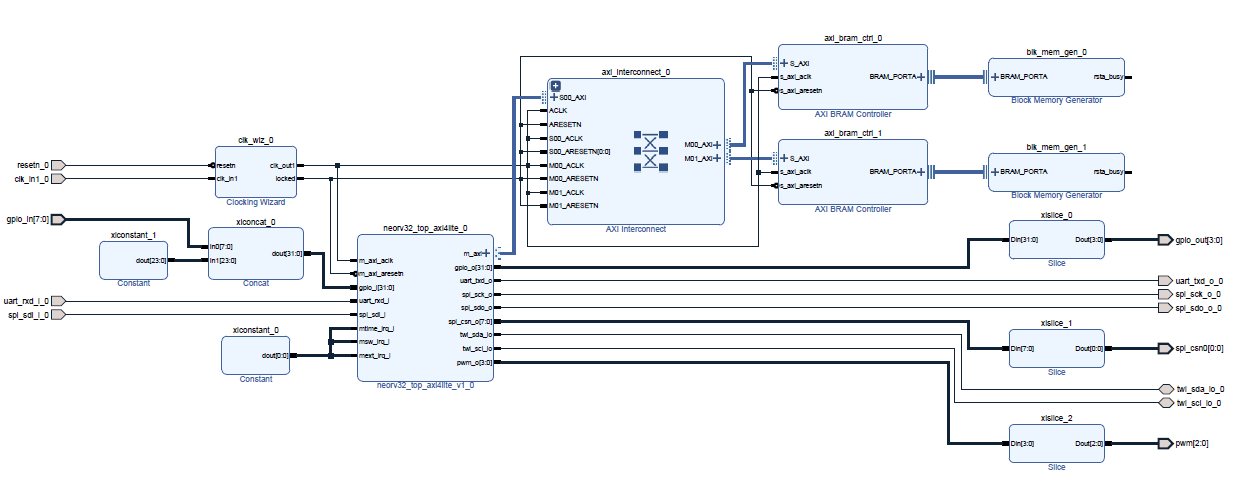
13. Packaging the Processor as IP block for Xilinx Vivado Block Designer
-
Import all the core files from
rtl/core(including default internal memory architectures fromrtl/core/mem) and assign them to a new design libraryneorv32. -
Instantiate the
rtl/wrappers/neorv32_top_axi4lite.vhdmodule. -
Then either directly use that module in a new block-design ("Create Block Design", right-click → "Add Module", thats easier for a first try) or package it ("Tools", "Create and Package new IP") for the use in other projects.
-
Connect your AXI-peripheral directly to the core’s AXI4-Interface if you only have one, or to an AXI-Interconnect (from the IP-catalog) if you have multiple peripherals.
-
Connect ALL the
ACLKandARESETNpins of all peripherals and interconnects to the processor’s clock and reset signals to have a unified clock and reset domain (easier for a first setup). -
Open the "Address Editor" tab and let Vivado assign the base-addresses for the AXI-peripherals (you can modify them according to your needs).
-
For all FPGA-external signals (like UART signals) make all the connections you need "external" (right-click on the signal/pin → "Make External").
-
Save everything, let VIVADO create a HDL-Wrapper for the block-design and choose this as your Top Level Design.
-
Define your constraints and generate your bitstream.
|
TWI Tri-State Drivers
Set the synthesis option "global" when generating the block design to maintain the internal TWI tri-state drivers.
|
Guide provided by GitHub user AWenzel83 (see
https://github.com/stnolting/neorv32/discussions/52#discussioncomment-819013). ❤️
|
14. Simulating the Processor
The NEORV32 project includes a core CPU, built-in peripherals in the Processor Subsystem, and additional peripherals in the templates and examples. Therefore, there is a wide range of possible testing and verification strategies.
On the one hand, a simple smoke testbench allows ensuring that functionality is correct from a software point of view. That is used for running the RISC-V architecture tests, in order to guarantee compliance with the ISA specification(s).
On the other hand, VUnit and Verification Components are used for verifying the functionality of the various peripherals from a hardware point of view.
14.1. Testbench
A plain-VHDL (no third-party libraries) testbench (sim/simple/neorv32_tb.simple.vhd) can be used for simulating and
testing the processor.
This testbench features a 100MHz clock and enables all optional peripheral and CPU extensions except for the E
extension and the TRNG IO module (that CANNOT be simulated due to its combinatorial (looped) architecture).
The simulation setup is configured via the "User Configuration" section located right at the beginning of the testbench’s architecture. Each configuration constant provides comments to explain the functionality.
Besides the actual NEORV32 Processor, the testbench also simulates "external" components that are connected to the processor’s external bus/memory interface. These components are:
-
an external instruction memory (that also allows booting from it)
-
an external data memory
-
an external memory to simulate "external IO devices"
-
a memory-mapped registers to trigger the processor’s interrupt signals
The following table shows the base addresses of these four components and their default configuration and properties:
|
Attributes:
|
| Base address | Size | Attributes | Description |
|---|---|---|---|
|
|
|
external IMEM (initialized with application image) |
|
|
|
external DMEM |
|
64 bytes |
|
external "IO" memory, atomic accesses will fail |
|
4 bytes |
|
memory-mapped register to trigger "machine external", "machine software" and "SoC Fast Interrupt" interrupts |
The simulated NEORV32 does not use the bootloader and directly boots the current application image (from
the rtl/core/neorv32_application_image.vhd image file).
|
|
UART output during simulation
Data written to the NEORV32 UART0 / UART1 transmitter is send to a virtual UART receiver implemented
as part of the testbench. Received chars are send to the simulator console and are also stored to a log file
(neorv32.testbench_uart0.out for UART0, neorv32.testbench_uart1.out for UART1) inside the simulation’s home folder.
Please note that printing via the native UART receiver takes a lot of time. For faster simulation console output
see section Faster Simulation Console Output.
|
14.2. Faster Simulation Console Output
When printing data via the UART the communication speed will always be based on the configured BAUD rate. For a simulation this might take some time. To have faster output you can enable the simulation mode for UART0/UART1 (see section Documentation: Primary Universal Asynchronous Receiver and Transmitter (UART0)).
ASCII data sent to UART0|UART1 will be immediately printed to the simulator console and logged to files in the simulator execution directory:
-
neorv32.uart?.sim_mode.text.out: ASCII data. -
neorv32.uart?.sim_mode.data.out: all written 32-bit dumped as 8-char hexadecimal values.
You can "automatically" enable the simulation mode of UART0/UART1 when compiling an application.
In this case, the "real" UART0/UART1 transmitter unit is permanently disabled.
To enable the simulation mode just compile and install your application and add UART?_SIM_MODE to the compiler’s
USER_FLAGS variable (do not forget the -D suffix flag):
sw/example/blink_led$ make USER_FLAGS+=-DUART0_SIM_MODE clean_all allThe provided define will change the default UART0/UART1 setup function in order to set the simulation mode flag in the according UART’s control register.
The UART simulation output (to file and to screen) outputs "complete lines" at once. A line is
completed with a line feed (newline, ASCII \n = 10).
|
14.3. Simulation using a shell script (with GHDL)
To simulate the processor using GHDL navigate to the sim/simple/ folder and run the provided shell script.
Any arguments that are provided while executing this script are passed to GHDL.
For example the simulation time can be set to 20ms using --stop-time=20ms as argument.
neorv32/sim/simple$ sh ghdl_sim.sh --stop-time=20ms14.4. Simulation using Application Makefiles (In-Console with GHDL)
To directly compile and run a program in the console (using the default testbench and GHDL
as simulator) you can use the sim makefile target. Make sure to use the UART simulation mode
(USER_FLAGS+=-DUART0_SIM_MODE and/or USER_FLAGS+=-DUART1_SIM_MODE) to get
faster / direct-to-console UART output.
sw/example/blink_led$ make USER_FLAGS+=-DUART0_SIM_MODE clean_all sim
[...]
Blinking LED demo program
14.4.1. Hello World!
To do a quick test of the NEORV32 make sure to have GHDL and a
[RISC-V gcc toolchain](https://github.com/stnolting/riscv-gcc-prebuilt) installed.
Navigate to the project’s sw/example/hello_world folder and run make USER_FLAGS+=-DUART0_SIM_MODE MARCH=rv32imac clean_all sim:
| The simulator will output some sanity check notes (and warnings or even errors if something is ill-configured) right at the beginning of the simulation to give a brief overview of the actual NEORV32 SoC and CPU configurations. |
stnolting@Einstein:/mnt/n/Projects/neorv32/sw/example/hello_world$ make USER_FLAGS+=-DUART0_SIM_MODE MARCH=rv32imac clean_all sim
../../../sw/lib/source/neorv32_uart.c: In function 'neorv32_uart0_setup':
../../../sw/lib/source/neorv32_uart.c:301:4: warning: #warning UART0_SIM_MODE (primary UART) enabled! Sending all UART0.TX data to text.io simulation output instead of real UART0 transmitter. Use this for simulations only! [-Wcpp]
  301 |   #warning UART0_SIM_MODE (primary UART) enabled! Sending all UART0.TX data to text.io simulation output instead of real UART0 transmitter. Use this for simulations only! (1)
      |    ^~~~~~~
Memory utilization:
   text    data     bss     dec     hex filename
   4612       0     120    4732    127c main.elf (2)
Compiling ../../../sw/image_gen/image_gen
Installing application image to ../../../rtl/core/neorv32_application_image.vhd (3)
Simulating neorv32_application_image.vhd...
Tip: Compile application with USER_FLAGS+=-DUART[0/1]_SIM_MODE to auto-enable UART[0/1]'s simulation mode (redirect UART output to simulator console). (4)
Using simulation runtime args: --stop-time=10ms (5)
../rtl/core/neorv32_top.vhd:347:3:@0ms:(assertion note): NEORV32 PROCESSOR IO Configuration: GPIO MTIME UART0 UART1 SPI TWI PWM WDT CFS SLINK NEOLED XIRQ (6)
../rtl/core/neorv32_top.vhd:370:3:@0ms:(assertion note): NEORV32 PROCESSOR CONFIG NOTE: Boot configuration: Direct boot from memory (processor-internal IMEM).
../rtl/core/neorv32_top.vhd:394:3:@0ms:(assertion note): NEORV32 PROCESSOR CONFIG NOTE: Implementing on-chip debugger (OCD).
../rtl/core/neorv32_cpu.vhd:169:3:@0ms:(assertion note): NEORV32 CPU ISA Configuration (MARCH): RV32IMACU_Zbb_Zicsr_Zifencei_Zfinx_Debug
../rtl/core/neorv32_cpu.vhd:189:3:@0ms:(assertion note): NEORV32 CPU CONFIG NOTE: Implementing NO dedicated hardware reset for uncritical registers (default, might reduce area). Set package constant <dedicated_reset_c> = TRUE to configure a DEFINED reset value for all CPU registers.
../rtl/core/neorv32_imem.vhd:107:3:@0ms:(assertion note): NEORV32 PROCESSOR CONFIG NOTE: Implementing processor-internal IMEM as ROM (16384 bytes), pre-initialized with application (4612 bytes).
../rtl/core/neorv32_dmem.vhd:89:3:@0ms:(assertion note): NEORV32 PROCESSOR CONFIG NOTE: Implementing processor-internal DMEM (RAM, 8192 bytes).
../rtl/core/neorv32_wishbone.vhd:136:3:@0ms:(assertion note): NEORV32 PROCESSOR CONFIG NOTE: External Bus Interface - Implementing STANDARD Wishbone protocol.
../rtl/core/neorv32_wishbone.vhd:140:3:@0ms:(assertion note): NEORV32 PROCESSOR CONFIG NOTE: External Bus Interface - Implementing auto-timeout (255 cycles).
../rtl/core/neorv32_wishbone.vhd:144:3:@0ms:(assertion note): NEORV32 PROCESSOR CONFIG NOTE: External Bus Interface - Implementing LITTLE-endian byte order.
../rtl/core/neorv32_wishbone.vhd:148:3:@0ms:(assertion note): NEORV32 PROCESSOR CONFIG NOTE: External Bus Interface - Implementing registered RX path.
../rtl/core/neorv32_slink.vhd:161:3:@0ms:(assertion note): NEORV32 PROCESSOR CONFIG NOTE: Implementing 8 RX and 8 TX stream links.
(7)
                                                                                       ##
                                                                                       ##         ##   ##   ##
 ##     ##   #########   ########    ########   ##      ##   ########    ########      ##       ################
####    ##  ##          ##      ##  ##      ##  ##      ##  ##      ##  ##      ##     ##     ####            ####
## ##   ##  ##          ##      ##  ##      ##  ##      ##          ##         ##      ##       ##   ######   ##
##  ##  ##  #########   ##      ##  #########   ##      ##      #####        ##        ##     ####   ######   ####
##   ## ##  ##          ##      ##  ##    ##     ##    ##           ##     ##          ##       ##   ######   ##
##    ####  ##          ##      ##  ##     ##     ##  ##    ##      ##   ##            ##     ####            ####
##     ##    #########   ########   ##      ##      ##       ########   ##########     ##       ################
                                                                                       ##         ##   ##   ##
                                                                                       ##
Hello world! :)| 1 | Notifier that "simulation mode" of UART0 is enabled (by the USER_FLAGS+=-DUART0_SIM_MODE makefile flag). All UART0 output is send to the simulator console. |
| 2 | Final executable size (text) and static data memory requirements (data, bss). |
| 3 | The application code is installed as pre-initialized IMEM. This is the default approach for simulation. |
| 4 | A note regarding UART "simulation mode", but we have already enabled that. |
| 5 | List of (default) arguments that were send to the simulator. Here: maximum simulation time (10ms). |
| 6 | "Sanity checks" from the core’s VHDL files. These reports give some brief information about the SoC/CPU configuration (→ generics). If there are problems with the current configuration, an ERROR will appear. |
| 7 | Execution of the actual program starts. |
14.5. Advanced Simulation using VUnit
VUnit is an open source unit testing framework for VHDL/SystemVerilog. It allows continuous and automated testing of HDL code by complementing traditional testing methodologies. The motto of VUnit is "testing early and often" through automation.
VUnit is composed by a Python interface and multiple optional
VHDL libraries.
The Python interface allows declaring sources and simulation options, and it handles the compilation, execution and
gathering of the results regardless of the simulator used.
That allows having a single run.py script to be used with GHDL, ModelSim/QuestaSim, Riviera PRO, etc.
On the other hand, the VUnit’s VHDL libraries provide utilities for assertions, logging, having virtual queues, handling CSV files, etc.
The Verification Component Library uses those features
for abstracting away bit-toggling when verifying standard interfaces such as Wishbone, AXI, Avalon, UARTs, etc.
Testbench sources in sim (such as sim/neorv32_tb.vhd and sim/uart_rx*.vhd) use VUnit’s VHDL libraries for testing
NEORV32 and peripherals.
The entry-point for executing the tests is sim/run.py.
# ./sim/run.py -l
neorv32.neorv32_tb.all
Listed 1 tests

# ./sim/run.py -v
Compiling into neorv32:   rtl/core/neorv32_uart.vhd                                                                                            passed
Compiling into neorv32:   rtl/core/neorv32_twi.vhd                                                                                             passed
Compiling into neorv32:   rtl/core/neorv32_trng.vhd                                                                                            passed
...
See VUnit: User Guide and VUnit: Command Line Interface for further info about VUnit’s features.
15. Building the Documentation
The documentation (datasheet + user guide) is written using asciidoc. The according source files
can be found in docs/…. The documentation of the software framework is written in-code using doxygen.
A makefiles in the project’s docs directory is provided to build all of the documentation as HTML pages
or as PDF documents.
| Pre-rendered PDFs are available online as nightly pre-releases: https://github.com/stnolting/neorv32/releases. The HTML-based documentation is also available online at the project’s GitHub Pages. |
The makefile provides a help target to show all available build options and their according outputs.
neorv32/docs$ make helpasciidoctorneorv32/docs$ make html
If you don’t have asciidoctor / asciidoctor-pdf installed, you can still generate all the documentation using
a docker container via make container.
|
16. Zephyr RTOS Support 🪁
The NEORV32 processor is supported by upstream Zephyr RTOS: https://docs.zephyrproject.org/latest/boards/riscv/neorv32/doc/index.html
The absolute path to the NEORV32 executable image generator binary (…/neorv32/sw/image_gen) has to be added to the PATH variable
so the Zephyr build system can generate executables and memory-initialization images.
|
| Zephyr OS port provided by GitHub user henrikbrixandersen (see https://github.com/stnolting/neorv32/discussions/172). ❤️ |
17. FreeRTOS Support
A NEORV32-specific port and a simple demo for FreeRTOS (https://github.com/FreeRTOS/FreeRTOS) are
available in the sw/example/demo_freeRTOS folder. See the according documentation (sw/example/demo_freeRTOS/README.md)
for more information.
18. RISC-V Architecture Test Framework
The NEORV32 Processor passes the according tests provided by the official RISC-V Architecture Test Suite (V2.0+), which is available online at GitHub: https://github.com/riscv/riscv-arch-test
All files required for executing the test framework on a simulated instance of the processor (including port
files) are located in the sw/isa-test folder of the NEORV32 repository. The test framework is executed via the
sim/run_riscv_arch_test.sh script. Take a look at the provided sim/README.md
(online at GitHub)
file for more information on how to run the tests and how testing is conducted in detail.
19. Debugging using the On-Chip Debugger
The NEORV32 on-chip debugger allows online in-system debugging via an external JTAG access port from a host machine. The general flow is independent of the host machine’s operating system. However, this tutorial uses Windows and Linux (Ubuntu on Windows) in parallel.
| See datasheet section On Chip Debugger (OCD) for more information. |
This tutorial uses gdb to directly upload an executable to the processor. If you are using the default
processor setup with internal instruction memory (IMEM) make sure it is implemented as RAM
(INT_BOOTLOADER_EN generic = true).
|
The on-chip debugger is only implemented if the ON_CHIP_DEBUGGER_EN generic is set true. Furthermore, it requires
the Zicsr and Zifencei CPU extension to be implemented (top generics CPU_EXTENSION_RISCV_Zicsr
and CPU_EXTENSION_RISCV_Zifencei = true).
|
19.1. Hardware Requirements
Make sure the on-chip debugger of your NEORV32 setups is implemented (ON_CHIP_DEBUGGER_EN generic = true).
Connect a JTAG adapter to the NEORV32 jtag_* interface signals. If you do not have a full-scale JTAG adapter, you can
also use a FTDI-based adapter like the "FT2232H-56Q Mini Module", which is a simple and inexpensive FTDI breakout board.
| NEORV32 top signal | JTAG signal | FTDI port |
|---|---|---|
|
TCK |
D0 |
|
TDI |
D1 |
|
TDO |
D2 |
|
TMS |
D3 |
|
TRST |
D4 |
| The low-active JTAG test reset (TRST) signals is optional as a reset can also be triggered via the TAP controller. If TRST is not used make sure to pull the signal high. |
19.2. OpenOCD
The NEORV32 on-chip debugger can be accessed using the RISC-V port of OpenOCD.
Prebuilt binaries can be obtained - for example - from SiFive. A pre-configured
OpenOCD configuration file (sw/openocd/openocd_neorv32.cfg) is available that allows easy access to the NEORV32 CPU.
You might need to adapt ftdi_vid_pid, ftdi_channel and ftdi_layout_init in sw/openocd/openocd_neorv32.cfg
according to your interface chip and your operating system.
|
If you want to modify the JTAG clock speed (via adapter speed in sw/openocd/openocd_neorv32.cfg) make sure to meet
the clock requirements noted in Documentation: Debug Transport Module (DTM).
|
To access the processor using OpenOCD, open a terminal and start OpenOCD with the pre-configured configuration file.
N:\Projects\neorv32\sw\openocd>openocd -f openocd_neorv32.cfg
Open On-Chip Debugger 0.11.0-rc1+dev (SiFive OpenOCD 0.10.0-2020.12.1)
Licensed under GNU GPL v2
For bug reports:
        https://github.com/sifive/freedom-tools/issues
1
Info : Listening on port 6666 for tcl connections
Info : Listening on port 4444 for telnet connections
Info : clock speed 1000 kHz
Info : JTAG tap: neorv32.cpu tap/device found: 0x0cafe001 (mfg: 0x000 (<invalid>), part: 0xcafe, ver: 0x0)
Info : datacount=1 progbufsize=2
Info : Disabling abstract command reads from CSRs.
Info : Examined RISC-V core; found 1 harts
Info :  hart 0: XLEN=32, misa=0x40801105
Info : starting gdb server for neorv32.cpu.0 on 3333
Info : Listening on port 3333 for gdb connections
OpenOCD has successfully connected to the NEORV32 on-chip debugger and has examined the CPU (showing the content of
the misa CSRs). Now you can use gdb to connect via port 3333.
19.3. Debugging with GDB
This guide uses the simple "blink example" from sw/example/blink_led as simplified test application to
show the basics of in-system debugging.
At first, the application needs to be compiled. We will use the minimal machine architecture configuration
(rv32i) here to be independent of the actual processor/CPU configuration.
Navigate to sw/example/blink_led and compile the application:
.../neorv32/sw/example/blink_led$ make MARCH=rv32i USER_FLAGS+=-g clean_all all|
Adding debug symbols to the executable
USER_FLAGS+=-g passes the -g flag to the compiler so it adds debug information/symbols
to the generated ELF file. This is optional but will provide more sophisticated information for debugging
(like source file line numbers).
|
This will generate an ELF file main.elf that contains all the symbols required for debugging.
Furthermore, an assembly listing file main.asm is generated that we will use to define breakpoints.
Open another terminal in sw/example/blink_led and start gdb.
The GNU debugger is part of the toolchain (see Software Toolchain Setup).
.../neorv32/sw/example/blink_led$ riscv32-unknown-elf-gdb
GNU gdb (GDB) 10.1
Copyright (C) 2020 Free Software Foundation, Inc.
License GPLv3+: GNU GPL version 3 or later <http://gnu.org/licenses/gpl.html>
This is free software: you are free to change and redistribute it.
There is NO WARRANTY, to the extent permitted by law.
Type "show copying" and "show warranty" for details.
This GDB was configured as "--host=x86_64-pc-linux-gnu --target=riscv32-unknown-elf".
Type "show configuration" for configuration details.
For bug reporting instructions, please see:
<https://www.gnu.org/software/gdb/bugs/>.
Find the GDB manual and other documentation resources online at:
    <http://www.gnu.org/software/gdb/documentation/>.

For help, type "help".
Type "apropos word" to search for commands related to "word".
(gdb)
Now connect to OpenOCD using the default port 3333 on your machine.
We will use the previously generated ELF file main.elf from the blink_led example.
Finally, upload the program to the processor and start debugging.
The executable that is uploaded to the processor is not the default NEORV32 executable (neorv32_exe.bin) that
is used for uploading via the bootloader. Instead, all the required sections (like .text) are extracted from mail.elf
by GDB and uploaded via the debugger’s indirect memory access.
|
(gdb) target extended-remote localhost:3333 (1)
Remote debugging using localhost:3333
warning: No executable has been specified and target does not support
determining executable automatically.  Try using the "file" command.
0xffff0c94 in ?? () (2)
(gdb) file main.elf (3)
A program is being debugged already.
Are you sure you want to change the file? (y or n) y
Reading symbols from main.elf...
(gdb) load (4)
Loading section .text, size 0xd0c lma 0x0
Loading section .rodata, size 0x39c lma 0xd0c
Start address 0x00000000, load size 4264
Transfer rate: 43 KB/sec, 2132 bytes/write.
(gdb)| 1 | Connect to OpenOCD |
| 2 | The CPU was still executing code from the bootloader ROM - but that does not matter here |
| 3 | Select mail.elf from the blink_led example |
| 4 | Upload the executable |
After the upload, GDB will make the processor jump to the beginning of the uploaded executable
(by default, this is the beginning of the instruction memory at 0x00000000) skipping the bootloader
and halting the CPU right before executing the blink_led application.
19.3.1. Breakpoint Example
The following steps are just a small showcase that illustrate a simple debugging scheme.
While compiling blink_led, an assembly listing file main.asm was generated.
Open this file with a text editor to check out what the CPU is going to do when resumed.
The blink_led example implements a simple counter on the 8 lowest GPIO output ports. The program uses
"busy wait" to have a visible delay between increments. This waiting is done by calling the neorv32_cpu_delay_ms
function. We will add a breakpoint right at the end of this wait function so we can step through the iterations
of the counter.
main.asm generated from the blink_led example00000688 <__neorv32_cpu_delay_ms_end>:
688: 01c12083 lw ra,28(sp)
68c: 02010113 addi sp,sp,32
690: 00008067 retThe very last instruction of the neorv32_cpu_delay_ms function is ret (= return)
at hexadecimal 690 in this example. Add this address as breakpoint to GDB.
| The address might be different if you use a different version of the software framework or if different ISA options are configured. |
(gdb) b * 0x690
Breakpoint 1 at 0x690|
How do breakpoints work?
The NEORV32 on-chip debugger does not provide any hardware breakpoints (RISC-V "trigger modules") that compare an address like the PC
with a predefined value. Instead, gdb will modify the actual executable in IMEM: the actual instruction at the address
of the specified breakpoint is replaced by a break / c.break instruction. Whenever execution reaches this instruction, debug mode is
re-entered and the debugger restores the original instruction at this address to maintain original program behavior.
|
Now execute c (= continue). The CPU will resume operation until it hits the break-point.
By this we can "step" from increment to increment.
Breakpoint 1 at 0x690
(gdb) c
Continuing.

Breakpoint 1, 0x00000690 in neorv32_cpu_delay_ms ()
(gdb) c
Continuing.

Breakpoint 1, 0x00000690 in neorv32_cpu_delay_ms ()
(gdb) c
Continuing.
20. Legal
License
BSD 3-Clause License
Copyright (c) 2021, Stephan Nolting. All rights reserved.
Redistribution and use in source and binary forms, with or without modification, are permitted provided that the following conditions are met:
-
Redistributions of source code must retain the above copyright notice, this list of conditions and the following disclaimer.
-
Redistributions in binary form must reproduce the above copyright notice, this list of conditions and the following disclaimer in the documentation and/or other materials provided with the distribution.
-
Neither the name of the copyright holder nor the names of its contributors may be used to endorse or promote products derived from this software without specific prior written permission.
THIS SOFTWARE IS PROVIDED BY THE COPYRIGHT HOLDERS AND CONTRIBUTORS "AS IS" AND ANY EXPRESS OR IMPLIED WARRANTIES, INCLUDING, BUT NOT LIMITED TO, THE IMPLIED WARRANTIES OF MERCHANTABILITY AND FITNESS FOR A PARTICULAR PURPOSE ARE DISCLAIMED. IN NO EVENT SHALL THE COPYRIGHT HOLDER OR CONTRIBUTORS BE LIABLE FOR ANY DIRECT, INDIRECT, INCIDENTAL, SPECIAL, EXEMPLARY, OR CONSEQUENTIAL DAMAGES (INCLUDING, BUT NOT LIMITED TO, PROCUREMENT OF SUBSTITUTE GOODS OR SERVICES; LOSS OF USE, DATA, OR PROFITS; OR BUSINESS INTERRUPTION) HOWEVER CAUSED AND ON ANY THEORY OF LIABILITY, WHETHER IN CONTRACT, STRICT LIABILITY, OR TORT (INCLUDING NEGLIGENCE OR OTHERWISE) ARISING IN ANY WAY OUT OF
The NEORV32 RISC-V Processor
Copyright (c) 2021, by Dipl.-Ing. Stephan Nolting. All rights reserved.
HQ: https://github.com/stnolting/neorv32
Contact: stnolting@gmail.com
made in Hanover, Germany
Proprietary Notice
-
"GitHub" is a Subsidiary of Microsoft Corporation.
-
"Vivado" and "Artix" are trademarks of Xilinx Inc.
-
"AXI", "AXI4-Lite" and "AXI4-Stream" are trademarks of Arm Holdings plc.
-
"ModelSim" is a trademark of Mentor Graphics – A Siemens Business.
-
"Quartus Prime" and "Cyclone" are trademarks of Intel Corporation.
-
"iCE40", "UltraPlus" and "Radiant" are trademarks of Lattice Semiconductor Corporation.
-
"Windows" is a trademark of Microsoft Corporation.
-
"Tera Term" copyright by T. Teranishi.
-
Timing diagrams made with WaveDrom Editor.
-
"NeoPixel" is a trademark of Adafruit Industries.
-
Documentation made with
asciidoctor.
PDF icons from https://www.flaticon.com and made by Freepik, Good Ware, Pixel perfect, Vectors Market
Disclaimer
This project is released under the BSD 3-Clause license. No copyright infringement intended. Other implied or used projects might have different licensing – see their documentation to get more information.
Limitation of Liability for External Links
This document contains links to the websites of third parties ("external links"). As the content of these websites is not under our control, we cannot assume any liability for such external content. In all cases, the provider of information of the linked websites is liable for the content and accuracy of the information provided. At the point in time when the links were placed, no infringements of the law were recognizable to us. As soon as an infringement of the law becomes known to us, we will immediately remove the link in question.
Citing
If you are using the NEORV32 or parts of the project in some kind of publication, please cite it as follows:
|
Contributors ❤️
Please add as many contributors as possible to the authors field 😉.This project would not be where it is without them. Full names can be found in the repository’s .mailmap.
|
@misc{nolting20,
  author       = {Nolting, S.},
  title        = {The NEORV32 RISC-V Processor},
  year         = {2020},
  publisher    = {GitHub},
  journal      = {GitHub repository},
  howpublished = {\url{https://github.com/stnolting/neorv32}}
}|
DOI
This project also provides a digital object identifier provided by zenodo:
|
Acknowledgments
A big shoutout to all contributors, who helped improving this project! ❤️
RISC-V - instruction sets want to be free!
Impressum (Imprint)
See docs/impressum.md.